On November 6, according to a report by foreign media outlet The Information, leading wafer foundry TSMC has recently begun planning a production scheme for 3D DRAM, and the direct force driving this decision comes from its largest customer, Nvidia. The memory shortage and price surge triggered by the AI computing power race are forcing Nvidia to seek supply paths beyond the three traditional memory giants, and TSMC has been pushed to the forefront.
If the plan materializes, TSMC will further enter the memory manufacturing field long dominated by Samsung, SK Hynix, and Micron, moving beyond logic chip foundry and advanced packaging. However, based on the available information, this looks more like a long-term game with technological reserves as the underlying card, customer pressure as the catalyst, and 2029 as the time anchor, rather than an imminent production line investment.
Nvidia's Anxiety, TSMC's Options
The report, citing two people familiar with the matter, disclosed that TSMC is considering expanding its business into the field of advanced memory chip manufacturing, and has, at the request of its largest customer Nvidia, begun an assessment of the feasibility of 3D DRAM production. This move is expected to enable TSMC to occupy a larger share of the AI hardware supply chain in the future.
3D DRAM is a memory architecture that increases capacity by vertically stacking memory cells (rather than the traditional horizontal single-layer arrangement). If the plan materializes, TSMC will compete with Samsung Electronics, SK Hynix, and Micron, the three manufacturers that have long dominated the memory market.
TSMC's specific options include building a dedicated new factory, or acquiring an existing semiconductor plant and converting it into a 3D DRAM production line. The latter path already has a precedent—Micron completed the acquisition of a wafer fab of Powerchip Semiconductor Manufacturing Corp in Taiwan, China for $1.8 billion in March this year, and plans to convert it for advanced memory chip production.
It is worth noting that this plan is led by Hsu Kuo-chin, TSMC's vice president responsible for advanced packaging technology. Hsu Kuo-chin previously served as chairman of Micron Taiwan, possessing a composite background in both memory manufacturing and chip integration. This arrangement implies that TSMC's consideration of the memory field is not a passing whim, but rather that a senior executive with industry experience is driving the feasibility demonstration.
Since last year, the continued booming AI wave has led to a severe shortage of memory chips and a sharp rise in prices. For Nvidia, the supply of high-bandwidth memory (HBM) required for its AI chips is highly concentrated among Samsung, SK Hynix, and Micron. Introducing TSMC as a potential supplier of a new type of memory is essentially seeking a "foundry-side" alternative path for the memory bottleneck of AI chips.
Regarding this news, TSMC's official response maintained its customary prudence: it does not comment on market rumors or speculation, and emphasizes that the company has always focused on its core wafer foundry business, with the goal of becoming a trusted technology and capacity supplier for the global logic chip industry.
Patents First, Roadmap Later
TSMC's technological accumulation in 3D DRAM presents a pattern in which "patent layout precedes the official roadmap."
According to the Korean media outlet Economy Tribune, which was the first to sort through TSMC's patent actions after the rumors fermented: TSMC applied for a US patent involving high-density 3D DRAM cells and capacitor structures in 2020, and in 2025 published a patent for a vertical DRAM structure and manufacturing method.
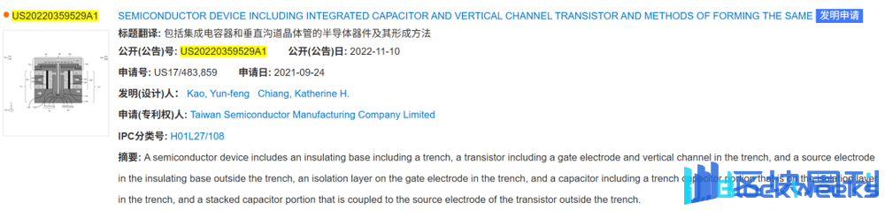
In addition, SemiWiki also mentioned in its analysis that TSMC has publicly applied for patents US20220359529A1 and US20230240066A1, which respectively describe integration schemes for vertical channel transistors and stacked capacitors.
After verifying the relevant patent databases, Core Intelligence News learned that patent US20220359529A1 was filed in September 2021 and describes an integrated structure of vertical channel transistors with hybrid trench and stacked capacitors, attempting to maintain sufficient capacitance while reducing the cell footprint; patent US20230240066A1 was filed in July 2023 and describes a vertical DRAM structure and its formation method. Its core scheme is to place the capacitor directly above a vertical gate-all-around (GAA) transistor and utilize back-end-of-line (BEOL) integration so that memory cells can be stacked layer by layer. The application also mentions design details such as a 4F² memory cell footprint, dual-layer bit line routing to reduce parasitic capacitance, and air gaps between word lines.


In addition, Core Intelligence News also found that TSMC's granted or pending 3D DRAM patents include US11903216B2 (granted in February 2024), which involves multiple patterning processes for three-dimensional memory devices; US20260333663A1 (filed in July 2026), which improves integration density and performance through transistor-level three-dimensional structure designs (such as Ω-shaped channel layers) while avoiding the complexity brought by capacitor manufacturing; US20240381657A1 (filed in November 2024), whose described three-dimensional memory array is composed of thin-film transistors (TFTs) with three-dimensional channel regions, and three-dimensional channel TFTs are precisely one of the key paths to realizing high-density 3D DRAM.


However, the above patent disclosures should be understood as technological exploration, rather than production readiness or a commercial DRAM commitment. Combining different patents into a single architecture, or inferring from them that TSMC is about to mass-produce 3D DRAM, lacks a basis.
However, a more indicative signal than the 3D DRAM-related patents comes from TSMC's own technology roadmap. In its analysis of TSMC's 2026 North America OIP Ecosystem Forum, Counterpoint Research noted that TSMC has included DRAM-on-logic in its 2029 roadmap, with the goal of achieving approximately 3 times the bandwidth of HBM5E at an energy consumption below 1 pJ/bit.
The technical implications of DRAM-on-logic align highly with 3D DRAM: manufacturing memory cells and logic circuits in separate layers and then vertically bonding them is precisely the core feature that distinguishes 3D DRAM from traditional DRAM. In other words, TSMC's potential advantage in 3D DRAM lies not in "making memory cells," but in "stacking logic and memory together in a high-density, low-power manner."
TSMC does indeed have a mass-production track record when it comes to "stacking" memory wafers. According to its annual report, its single-layer memory wafer stacking technology under its 55nm logic process has entered stable mass production. However, stacking completed DRAM wafers and building vertically repeating memory cells inside the memory array are two different things. TSMC is more focused on the former (HBM base logic die, CoWoS packaging), where its role is foundry and packaging, and it has very little practical experience in the latter.
The 3D DRAM Race Among the Three Memory Giants
If TSMC really enters the fray, it will face a group of competitors that have already been running on the 3D DRAM track for several years.
Samsung's roadmap is the clearest: 4F² vertical channel transistors will be used continuously across three generations of nodes, 10a, 10b, and 10c, and only at the 10d node will it shift to 3D stacked DRAM. In February 2026 at ISSCC, it already showcased a 16Gb 4F² DRAM prototype; 10a is planned to complete development in 2026, undergo quality testing in 2027, and enter mass production in 2028. Samsung has internally completed validation of 16-layer 3D DRAM stacking, and in the future memory cells and peripheral circuits will be manufactured separately and then integrated through hybrid bonding.
SK Hynix has listed 3D DRAM as a core R&D direction for DRAM below 10 nanometers, and at VLSI 2025 its CTO personally released the 4F² vertical gate platform and the 3D DRAM roadmap.
Micron, after evaluating 4F² technology for more than twenty years, concluded that "there is no practical benefit along this direction," and therefore plans to skip 4F² and rely on the continuity of the 6F² architecture to last until 3D DRAM matures. Micron has placed 3D DRAM in its technology planning between the 1ζ (1-zeta) and 1η (1-eta) nodes. However, Micron specifically emphasizes that 3D DRAM is in fact a parallel R&D route, rather than an established plan to immediately replace traditional DRAM at a certain node.
What these three major DRAM manufacturers have in common is: their accumulated engineering experience in DRAM manufacturing, yield control, cost optimization, and capacity ramp-up are things TSMC will find difficult to replicate in the short term. The vertical stacking structure of 3D DRAM further increases manufacturing complexity; for example, the more stacked layers there are, the higher the yield risk in etching, deposition, and bonding steps. If TSMC builds production lines from scratch, it could take several years from equipment installation to stable mass production.
In addition, the strong cyclicality of the memory industry is another concern. Historically, memory shortages often trigger manufacturers to rush into capacity expansion, and by the time the new capacity comes online, demand may already have fallen back. As a foundry company whose gross margin has long remained above 50%, whether TSMC is willing to bear the potentially severe profit fluctuations of the memory business remains uncertain. Moreover, memory prices have always been highly volatile, building new fabs requires huge capital, and capacity may take years to reach the market; whether TSMC will ultimately implement the plan has not yet been decided.
Conclusion:
For TSMC, the wisest course of action may not be to become the fourth memory manufacturer, but rather to use its "logic + packaging" capabilities to become an indispensable integrator in the 3D DRAM era. In other words, memory cells can be manufactured by third parties, but bonding memory and logic together with the lowest power consumption and highest bandwidth is something TSMC is better at than anyone else. As for whether it is willing to take another step forward for Nvidia and truly enter 3D DRAM manufacturing, that remains to be seen.
This article comes from the WeChat public account: Core Intelligence News , editor: Core Intelligence News - Langkejian, author: Core Intelligence News Langkejian